|
|
Manufacturing Capability
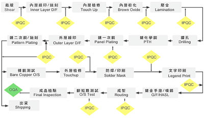
In-Process Control Chart
Outgoing Quality Assurance Case Timetable
PCB
We keep holding a consistent
persistence of specialty and design on work of PCB manufacturing, not
because of CAST consideration, but of board production, basic system
regulation requirements and quality. With the option to cooperate with
the board manufacturer to come up with the best solution for cost and
quality.
Manufacturing Capability
Technology
Description
Now
Under
Development
Minimum
Trace/Space (inner/outer)
5/5 mils
4/4 mils
Minimum
Finished Hole Diameter
10 mils
6 mils
Maximum
Aspect Ratio
8:1
10:1
Minimum
Board Thickness - 4 Layer
16 mils
12 mils
Minimum
Board Thickness - 6 Layer
24 mils
22 mils
Maximum
Board Thickness
125 mils
125 mils
Minimum/Maximum
Layer
2/16
up to 20
Minimum
SMT Device Pitch
12 mils
10 mils
Minimum
SMT Device Land Width
8 mils
6 mils
Board
Flatness Tolerance
±0.7%
±0.5%
Layer to
Layer Reg. Tolerance
±5 mils
±4 mils
Impedance
Control
Partial
Full
Entek /
Gold Plating
Yes
Yes
Board
Size
20" *
20"
24"
* 24"
In-Process Control Chart
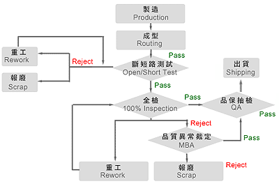
Outgoing Quality Assurance
Case Timetable Classification/Layer |
|
ADD: 10F.-2, No.192, Sec. 2, Zhongxing Rd., Xindian Dist., New Taipei City 23146, Taiwan (R.O.C.) TEL: 886-2-29113596 ext 100 All right reserved by Mouse-Team |


